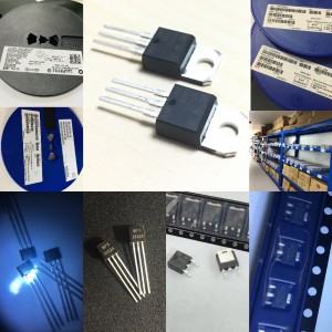
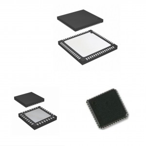
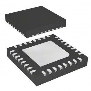
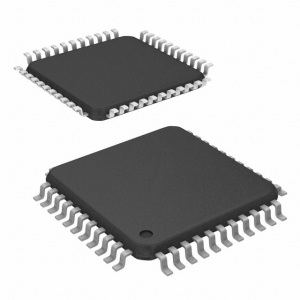
C8051F020-GQR IC MCU 8BIT 64KB FLASH 100TQFP
Product Parameter
Description
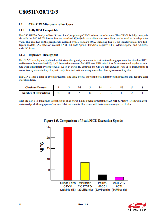
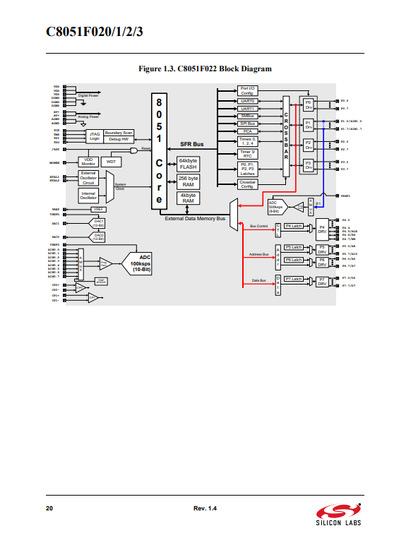
With on-chip VDD monitor, Watchdog Timer, and clock oscillator, the C8051F020/1/2/3 devices are truly standalone System-on-a-Chip solutions. All analog and digital peripherals are enabled/disabled and configured by user firmware. The FLASH memory can be reprogrammed even in-circuit, providing non-volatile data storage, and also allowing field upgrades of the 8051 firmware. On-board JTAG debug circuitry allows non-intrusive (uses no on-chip resources), full speed, in-circuit debugging using the production MCU installed in the final application. This debug system supports inspection and modification of memory and registers, setting breakpoints, watchpoints, single stepping, run and halt commands. All analog and digital peripherals are fully functional while debugging using JTAG. Each MCU is specified for 2.7 V-to-3.6 V operation over the industrial temperature range (-45° C to +85° C). The Port I/Os, /RST, and JTAG pins are tolerant for input signals up to 5 V. The C8051F020/2 are available in a 100-pin TQFP package (see block diagrams in Figure 1.1 and Figure 1.3). The C8051F021/3 are available in a 64-pin TQFP package (see block diagrams in Figure 1.2 and Figure 1.4).
| Specifications: | |
| Attribute | Value |
| Category | Integrated Circuits (ICs) |
| Embedded - Microcontrollers | |
| Mfr | Silicon Labs |
| Series | C8051F02x |
| Package | Tape & Reel (TR) |
| Part Status | Not For New Designs |
| Core Processor | 8051 |
| Core Size | 8-Bit |
| Speed | 25MHz |
| Connectivity | EBI/EMI, SMBus (2-Wire/I²C), SPI, UART/USART |
| Peripherals | Brown-out Detect/Reset, POR, PWM, Temp Sensor, WDT |
| Number of I/O | 64 |
| Program Memory Size | 64KB (64K x 8) |
| Program Memory Type | FLASH |
| EEPROM Size | - |
| RAM Size | 4.25K x 8 |
| Voltage - Supply (Vcc/Vdd) | 2.7V ~ 3.6V |
| Data Converters | A/D 8x8b, 8x12b; D/A 2x12b |
| Oscillator Type | Internal |
| Operating Temperature | -40°C ~ 85°C (TA) |
| Mounting Type | Surface Mount |
| Package / Case | 100-TQFP |
| Supplier Device Package | 100-TQFP (14x14) |
| Base Product Number | C8051F020 |
Related PRODUCTS
-

Tel
-

E-mail
-

skype
-

whatsapp
whatsapp


