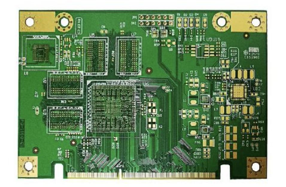
PCB surface treatment is the key and foundation of SMT patch quality. The treatment process of this link mainly includes the following points. Today, I will share the experience in the professional circuit board proofing with you:
(1) Except for ENG, the thickness of the plating layer is not clearly specified in the relevant national standards of PC. It is only required to meet the solderability requirements. The general requirements of the industry are as follows.
OSP: 0.15~0.5 μm, not specified by IPC. Recommended to use 0.3 ~ 0.4um
EING: Ni-3~5um; Au-0.05~0.20um (PC only stipulates the current thinnest requirement)
Im-Ag: 0.05~0.20um, the thicker, the more severe the corrosion is (PC not specified)
Im-Sn: ≥0.08um. The reason for thicker is that Sn and Cu will continue to develop into CuSn at room temperature, which affects solderability.
HASL Sn63Pb37 is generally formed naturally between 1 and 25um. It is difficult to accurately control the process. Lead-free mainly uses SnCu alloy. Due to the high processing temperature, it is easy to form Cu3Sn with poor sound solderability, and it is barely used at present.
(2) The wettability to SAC387 (according to the wetting time under different heating times, unit: s).
0 times: im-sn (2) florida ageing (1.2), osp (1.2) im-ag (3).
Zweiter PLENAR SESSION Zweiter PLENAR SESSION Im-Sn has the best corrosion resistance, but its solder resistance is relatively poor!
4 times: ENG (3)-ImAg (4.3)-OSP (10)-ImSn (10).

(3) The wettability to SAC305 (after passing through the furnace twice).
ENG (5.1)—Im-Ag (4.5)—Im-Sn (1.5)—OSP (0.3).
In fact, amateurs may be very confused with these professional parameters, but it must be noted by the manufacturers of PCB proofing and patching.
Post time: May-28-2021


